



Huawei Technologies says it is applying parts of its Tau Scaling Law, a chip-design principle it introduced in May, to the next generation of its wireless base stations, according to a South China Morning Post report published October 28. Lens could not open that article, because the site returned an access error, so the base-station details below rest on descriptions of the report and of a Huawei statement it cites. None of the material Lens reviewed contains independent measurements of the gains Huawei claims.
The step extends a framework that Huawei first presented as a way to keep improving semiconductors without relying only on smaller transistors. The newspaper’s headline frames the base-station rollout as a blow to US chip curbs. That framing is the newspaper’s, and the sources Lens could open do not show that the work gets around any US restriction.
What Huawei says about base stations
As described in summaries of the SCMP report, Huawei is using a time-compression concept drawn from the Tau Scaling Law in its next-generation base stations. The company says this already improves performance and efficiency.
Fang Xiang, a Huawei vice president and director of the company’s Wireless Network Business Management Committee, spoke about the work at an event called Decoding China 2026, according to those descriptions. He said Huawei uses the law in base-station design so that resources can be scheduled dynamically across a whole network, which should eventually ease capacity limits.
A Huawei statement cited in the coverage says the company is the first to bring the Tau law into base-station architecture. It names the problem as capacity limits caused by interference across frequencies, cells and users. The same account says Huawei’s latest UBBPi baseband products, which use the time-compression idea, deliver a 1.3-fold gain in average network experience and 40 percent lower energy use.
Those figures come from Huawei, and Lens could not check them against the original report. None of the material Lens reviewed explains how time compression is carried out in base-station hardware or software, or how much of any gain comes from the Tau principle rather than from other changes to the products.
Where the Tau Scaling Law came from
He Tingbo, chair of Huawei’s Scientist Committee and president of its semiconductor business department, presented the law on May 25 in a keynote at the 2026 IEEE International Symposium on Circuits and Systems in Shanghai, according to Yicai and KrASIA. Yicai describes it as a proposal to replace geometric scaling, the shrinking of transistors, with time scaling as the principle that guides how semiconductors and electronic systems develop.
Huawei’s argument is that Moore’s Law now faces severe physical limits and diminishing economic returns, as Yicai and Intelligent CIO report the company’s position. Under the Tau approach, progress is measured by how much the time constant, written as the Greek letter tau, can be reduced. In practice that means cutting signal delay. KrASIA quotes He as saying: “Losing geometric scaling does not mean losing time scaling.”
Huawei says the effort works at four levels at once, according to Telco Magazine and Intelligent CIO. At the device level it lowers resistance and parasitic capacitance in transistors and interconnects. At the circuit level it uses LogicFolding to shorten the wiring along critical signal paths. At the chip level it designs software, architecture and silicon together. At the system level it uses an interconnect protocol called UnifiedBus, which Huawei says gives unified memory addressing across large AI computing clusters it calls SuperPoDs.
LogicFolding and the density claims
LogicFolding is the technology Huawei puts at the center of the program. Yicai describes it as an architecture that moves from single-layer to double-layer logic. Telco Magazine reports that Huawei compares it to replacing a single-story building with a multi-story one, stacking circuit layers vertically so that signals travel shorter distances.
KrASIA reports figures He gave in the keynote. Before LogicFolding, transistor density rose from 126 million to 155 million per square millimeter over three years. In 2026, LogicFolding reaches 238 million per square millimeter in one step, according to those figures. Huawei has not published the underlying measurements in the sources Lens opened.
Yicai reports that the Kirin chips due this fall will be the first mass-produced product to use LogicFolding. Huawei also says it expects its high-end chips based on the law to reach a transistor density equivalent to a 14-angstrom, or 1.4-nanometer, process by 2031. KrASIA and CRN Asia both stress that this means equivalent density reached through architecture and circuit design, not true 1.4-nanometer lithography. For comparison, KrASIA notes that TSMC unveiled its 1.4-nanometer-class A14 process in 2025 and plans production in 2028.
Huawei further says it has designed and mass-produced 381 chips over six years using the principle, for smartphones, AI computing and other markets. Telco Magazine reports the 381 figure and separately says Huawei designs and mass-produces hundreds of such chips, without clarifying how many are in production.
The export-control backdrop
CRN Asia writes that US export restrictions have effectively cut China off from the advanced lithography equipment that TSMC and Samsung use for frontier chips, and it presents the Tau law and LogicFolding as Huawei’s response to that constraint. KrASIA says the approach could reduce reliance on the most advanced lithography tools but not eliminate it, and that export controls limit China’s near-term ability to make chips beyond 7 nanometers.
CRN Asia also lists Huawei’s Ascend AI chip schedule: the Ascend 950 series in 2026, the Ascend 960 in 2027 and the Ascend 970 in 2028. The same article reports that shares of the Chinese chipmaker SMIC rose 7.6 percent on the Monday after the keynote, and reads that as investors seeing industrial progress rather than speculation. Lens did not verify the share move independently.
Lens analysis: a base station is a different kind of test from a phone chip. Huawei sells base stations to network operators, who can measure capacity and energy use in their own trials. That gives the wireless claims a route to outside verification that the chip-density claims will not have until devices built on LogicFolding are on sale and can be taken apart and measured.
What has not been shown
Telco Magazine, in its May coverage of the keynote, linked the Tau approach to telecom through latency-sensitive uses such as AI-assisted radio access networks, real-time analytics, cloud-native telecom services and distributed edge computing. It named no telecom-specific chip, deployment or customer. It also noted that nearly all performance claims came from Huawei and that the article contained no independent analysts, third-party benchmarks or measured speed and energy figures.
Yicai’s report on the keynote likewise gives few technical details and no independent verification, and CRN Asia quotes no outside analysts. The 2031 density target and the 381-chip count are both Huawei’s own statements. The Kirin launch the company has scheduled for this fall is the first public product test of the density claims.
What to watch
The first checkpoint is the Kirin launch. Independent teardowns and density measurements of a chip built with LogicFolding would show whether the 238 million figure holds in a shipping product. Without them, the numbers remain presentation slides.
For the wireless business, the useful evidence would be operator-run trials or third-party measurements of the UBBPi products, with the baseline named and the share attributable to the Tau-based design separated from other changes. Huawei has not yet published such a breakdown in the material Lens reviewed.
A further question is how much technical detail Huawei releases. The company framed the law as a call for openness and collaboration, and Yicai, Telco Magazine and Intelligent CIO all report that emphasis, including the point that no single company can find every answer on the path of semiconductor evolution. Publishing methods and measurements would let outside engineers test the principle that the base-station announcement now extends.
Sources
- Yicai Global: Huawei Proposes Tau Scaling Law to Replace Moore’s Law in Chip Industry
- KrASIA: Huawei proposes Tau scaling law to extend chip advances beyond Moore’s law
- Telco Magazine: How Huawei’s Tau Scaling Law Reinvents Telco Chip Design
- CRN Asia: Huawei bets on a new law of physics to outmaneuver chip restrictions
- Intelligent CIO APAC: Huawei’s Tau (τ) Scaling Law ushers in a new era for transistor density and system performance
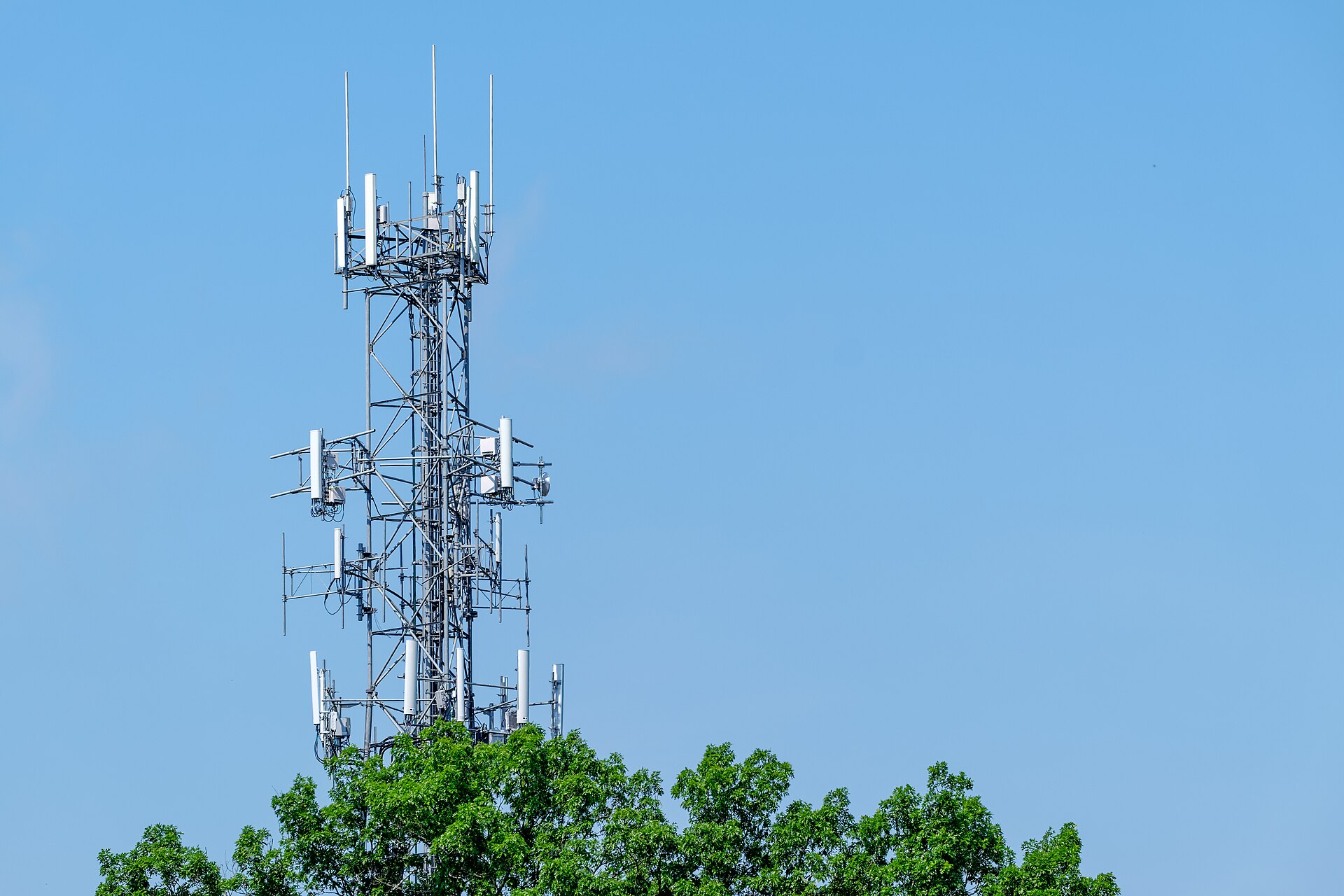
Image: Cellular Telephone Tower - Knoxville, Tennessee - May 26, 2014.jpg by David Ratledge, CC BY 4.0, via Wikimedia Commons. Illustrative photo; it does not show the events described.


