China's 300-mm Silicon Carbide Wafer Breakthrough Signals New Era in Semiconductor Manufacturing

China’s Game-Changing Launch: 300-mm Silicon-Carbide (SiC) Wafers Signal Major Industry Shift
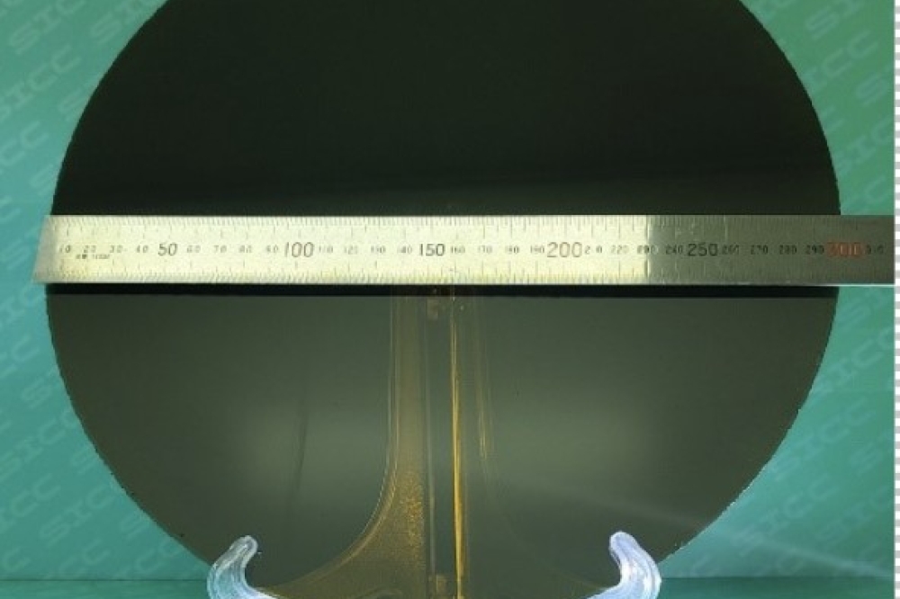
Breakthrough in Domestic Semiconductor Engineering
China’s semiconductor sector has set a new benchmark with the operational start of its first production line dedicated to manufacturing large-format silicon-carbide substrates, marking a pivotal moment for the industry. Zhejiang Jingsheng Mechanical & Electrical spearheads this initiative by developing the full production process in-house, utilizing entirely indigenous technology and locally made equipment at every step. This move underscores the nation's rapid technological advancement and determination to control the entire manufacturing value chain for advanced electronic materials.
Unlike previous dependence on imported tools and know-how, the process now relies on homegrown expertise, allowing Chinese engineers to refine key stages such as crystal growth, defect minimization, slicing, and surface inspection. The arrival of 300-mm substrates, which far surpass the area of traditional 150-mm and 200-mm wafers, is transforming efficiency benchmarks. By offering a platform with 2.5 times the chip output per substrate, the transition enhances cost-effectiveness while establishing a foundation for scalable mass production.
Impact on Cost Structure and Industrial Applications
A major advantage of shifting to larger SiC substrates lies in the economic ramifications for device manufacturers and end-users. The process reduces operational costs, with each substrate requiring significantly less handling and processing per device, leading to a 40% decrease in overall expenditure. Notably, for automotive systems that increasingly rely on SiC-based components, the price per unit is poised to drop from $150 to just $90. This cost-saving is crucial for the adoption of advanced electric vehicle designs, making cutting-edge technologies more accessible across commercial fleets and consumer markets.
Beyond automotive uses, the enhanced substrate format is strategically important to sectors fueling digital transformation. Markets for 5G infrastructure require high-performance, reliable materials with excellent thermal properties, while solar energy projects benefit from the increased durability and lower operational barriers presented by improved SiC modules. The expanded substrate size facilitates large-scale integration in both high-voltage energy solutions and next-generation network installations, amplifying their impact on global sustainability goals and communication advancements.
Global Market Position and Industry Implications
This manufacturing leap is reshaping the competitive dynamics in the global supply landscape. According to projections, the proportion of components supplied by Chinese firms in this domain is set to rise dramatically, with market share estimates jumping from one-fourth to over half within the year. This shift carries significant downstream implications for supply chain reliability, pricing policies, and international trade flows, especially as major manufacturers seek alternatives to traditional international wafer suppliers.
Industry observers note that the new substrates not only address challenges of defect control and production scalability but also set the stage for further technological evolution. The substrate’s performance metrics and yield consistency influence both design flexibility and market adaptability for chipmakers. As the production model matures and quality benchmarks continue to improve, these advances are expected to accelerate broader adoption by device firms and spur further innovation in related semiconductor domains.
Keywords
Silicon Carbide, 300-mm Wafer, Semiconductor Manufacturing, Automotive Components, Electric Vehicle Technology, 5G Infrastructure, Solar Energy Materials, Domestic Production