


ASML’s China Dip, Five Levels Down: What Beijing’s Lithography Push Actually Changes

ASML’s shares have had a rough patch, and Chinese lithography is part of the reason. But the stock moves and the machines are two separate stories, and the engineering explains why the market reacts quickly to one while the other will take years to matter. This piece goes down five levels, from the headline to the physics.
Level 1: What actually happened
The sharpest China-driven fall came on 27 July, when The Information reported that a Chinese company had begun manufacturing immersion deep-ultraviolet (DUV) lithography machines. ASML fell as much as 8% that Monday, according to CNBC. Reuters, following up the next day, put the two-day loss at about 10%, more than €60 billion of market value. Other outlets reported anywhere from 6% to 11%, depending on the day and the listing.
The maker is named differently depending on the outlet. Reuters identified Shanghai Aishengna Electronic Technology Group, a state-owned company; other coverage ties the tool to Shanghai Yuliangsheng Technology, a start-up linked to Huawei and to SiCarrier. Public reporting does not settle whether these are the same entity. The reported plan is five machines in 2026 and about 20 in 2027, for chipmakers such as SMIC.
October added more noise. On 14 October ASML reported third-quarter net sales of €11.7 billion, and the shares slipped on a slight miss and a softer margin outlook, by between about 2% and 5% depending on the outlet. Around the same time, a Shanghai start-up, Langdao Silex, showed a prototype EUV light source at the China International Industry Fair. On 22 October ASML closed down 6.9% in a chip-equipment selloff after Lam Research said supply constraints cap its outlook. On 30 October it fell 6.6% to $1,565.90 in US trading, from a $1,675.70 close, as the sector fell again. TradingKey put its sector down 4.2% and cited profit-taking; the automated MarketBeat alert gave no cause. None of the coverage reviewed for this piece ties either October fall to a Chinese announcement.
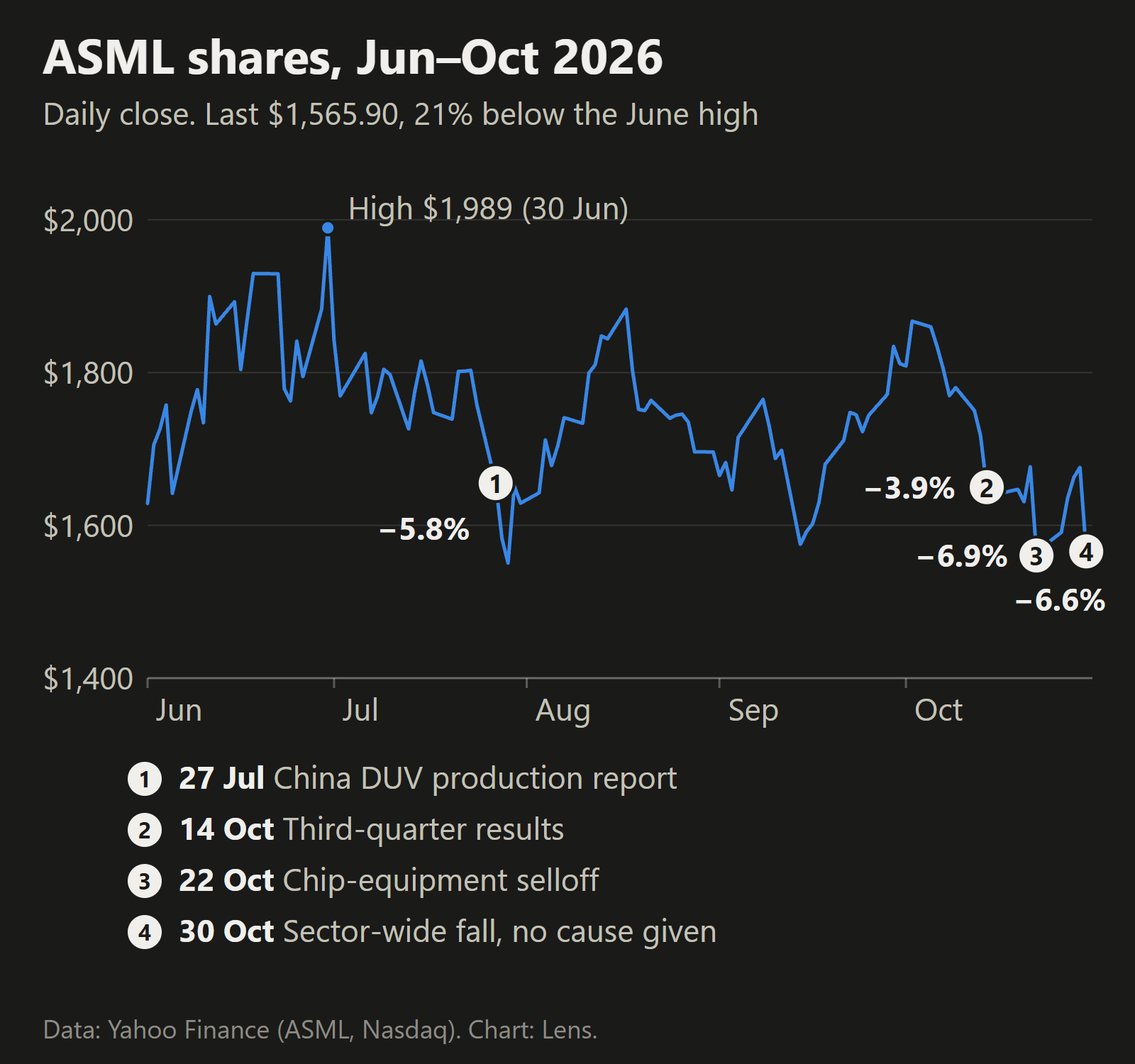
So one fall, in July, was a direct reaction to Chinese tool production. The October declines mix earnings, sector-wide selling and valuation. The useful question is what these machines would have to do to hurt ASML, and how far they are from doing it.
Level 2: Two kinds of machine
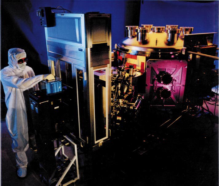
Lithography prints a chip’s patterns onto a wafer with light. ASML sells two families. Immersion DUV uses 193 nm argon-fluoride lasers, with a film of water between the last lens and the wafer. EUV uses 13.5 nm light and, because no lens material passes it, steers that light with mirrors in a vacuum.
The Chinese tool reported in July is the first kind. Export rules already bar ASML from selling its most advanced EUV machines and its best immersion tools in China, though older immersion systems still ship. That gap is what a domestic tool targets. Sanne van der Lugt of the Leiden Asia Center told Reuters that “U.S. export controls successfully created a business case for Chinese lithography,” adding: “For Chinese customers it may be this or nothing.”
Scale matters too. ASML shipped 131 immersion systems in 2025 and, per CNBC, plans capacity of about 130 in 2026 with 30% more in 2027, roughly 170. Twenty Chinese tools in 2027 would be about 12% of that. It is a rounding error for the world market and a lifeline inside China.
Level 3: The optics equation
The smallest feature a scanner can print in one exposure follows the Rayleigh relation: half-pitch = k1 × wavelength ÷ numerical aperture (NA). Immersion matters because water, with a refractive index of about 1.44 at 193 nm, lets the lens gather light at steeper angles than air, which caps NA below 1.0. The NXT:1950i, the 2008 ASML machine that Tom’s Hardware, citing the Financial Times, said the Chinese tool resembles, reaches an NA of 1.35.
Do the arithmetic: 193 ÷ 1.35 is about 143 nm. The theoretical single-exposure limit is k1 = 0.25, or about 36 nm. The 38 nm resolution quoted for the 1950i implies a k1 of about 0.27, close to that wall. One pass through a machine of this class simply cannot print denser lines.
The workaround is multipatterning: split a dense pattern across two or more masks and exposures, or use deposited spacers to double or quadruple line density. The Chinese tool is reportedly designed for 28 nm-class manufacturing and could in principle reach 7 nm or 5 nm-class with multipatterning, but Tom’s Hardware noted that “it remains to be seen” whether that works without big gains in overlay, precision and control. (Node names such as “7 nm” are marketing labels, not feature sizes.) The same report expects sub-10 nm output on domestic lithography to be unlikely before 2030.
Multipatterning also has a price that the node name hides. Each extra pass is another mask, another exposure, another trip through the track and the etcher, and another chance to put a line in the wrong place. A layer that one EUV exposure prints in a single step may take two, three or four immersion passes. That is why chipmakers with access to EUV use it for their tightest layers: not because immersion cannot reach the pattern, but because the cost and the defects add up per pass.
Level 4: The machine around the lens
A lens that resolves 38 nm is the easy part to specify. The hard part is placing the second exposure on top of the first to within a few nanometres across a 300 mm wafer. That is overlay. The overlay cited for the 1950i is 2.5 nm, about 7% of a 38 nm half-pitch. In a multipatterned layer the errors of separate passes combine, roughly in quadrature, and every nanometre of slack is paid for in yield. ASML’s current NXT:2100i is a dual-stage system, one stage exposing while the other measures, and ASML says it improved single-machine overlay by up to 10% and matched-machine overlay by 13% over its predecessor, with alignment measurements raised from 4 to 12 colours.
“Matched-machine” is the phrase to notice. A fab runs dozens of scanners that must agree with each other to the nanometre, so a vendor sells a fleet that stays calibrated for years, not one tool that works once. For the Chinese machine, no throughput, overlay or uptime figures have been published. Nick Patience of Futurum told CNBC: “They need to get to at least yield parity, not just have a working tool.” SemiAnalysis said scaling production of the machine itself is “the most underestimated part” and flagged “poor economics against fully depreciated ASML machines.” JPMorgan’s analysts wrote that producing a handful of immersion tools is not the same as building equipment for high-volume manufacturing.
There is also the question of what is inside the box. The Chinese tool is reportedly made mostly from Chinese components, though some parts are still imported, and the supply chain is being localised on a timetable nobody has published. Lenses polished to sub-nanometre accuracy, stages that move a wafer at high speed and stop within nanometres, and lasers that stay stable for months are each a company’s life work. A tool is only as good as its weakest subsystem, and each one has to be built and then matched to the others.
Level 5: The light
EUV is where the physics gets unforgiving. ASML’s source ejects molten tin droplets about 25 microns across at 70 metres per second, 50,000 times a second. A weak laser pulse first flattens each droplet into a pancake; a much stronger pulse then vaporises it into a plasma that emits 13.5 nm light.
Why power matters comes down to photon counting. A 13.5 nm photon carries about 92 eV, roughly 14 times the 6.4 eV of a 193 nm photon. At an illustrative dose of 30 mJ/cm², that is about 20 EUV photons per square nanometre against roughly 290 at 193 nm. In a 10 nm by 10 nm patch, about 2,000 EUV photons arrive, and their random arrival alone produces around 2% dose noise. That noise shows up as rough edges and, now and then, a contact that fails to open: stochastic defects. Raising the dose cures it, but dose costs source power.
Power also sets throughput. Exposing a 300 mm wafer (about 707 cm²) at 30 mJ/cm² takes roughly 21 J. At 125 wafers an hour, the rate ASML reached with a 250 W source in 2018, that averages about 0.74 W delivered to the wafer, around 0.3% of the source power: the roughly dozen reflective surfaces in the optical path, the mask included, each lose around a third of the light, and the time spent loading and aligning wafers takes the rest. (This is illustrative arithmetic, not ASML data.)
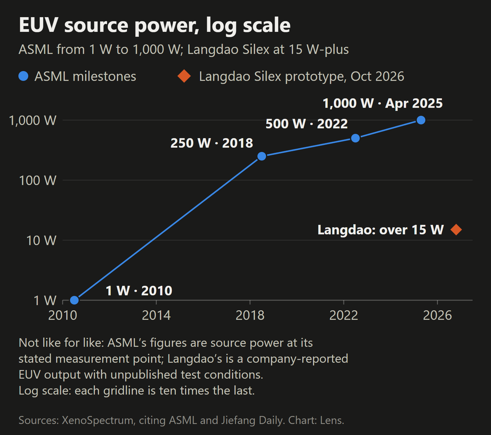
ASML’s source went from 1 W in an early 2010 prototype to 250 W in 2018, a 500 W prototype in 2022 and a 1,000 W demonstration in April 2025. Langdao Silex’s FlintNano LPP-OXXO, shown in Shanghai in mid-October, uses a 1,000 W drive laser at 1 to 20 kHz and claims a conversion efficiency above 2%, an EUV output above 15 W and more than 100 hours of continuous operation. Staff put mass production three to five years away and domestic content at 90%.
Read those numbers carefully. Fifteen watts is about one-seventeenth of the 250 W ASML had in 2018, but the two figures are not measured at the same point, and the 1,000 W is laser input, not EUV output. The company has not published its measurement conditions or long-term stability, and Tom’s Hardware noted that the source has not been demonstrated in action. Its repetition rate of up to 20 kHz is also well below ASML’s 50,000 droplets a second. And a light source is not a scanner: the mirrors, the stage, the mask handling and the chemistry of the resist all remain.
One more number puts the 100 hours in context. The plasma and tin debris erode a source’s collector mirror, and a public-domain chart by I. Fomenkov, showing data for two generations of EUV sources, shows how fast: reflectivity falls to roughly 70% by 100 gigapulses and to about a third by 200. At ASML’s 50 kHz, 100 gigapulses is about 23 days of firing. Langdao’s 100 hours at its top repetition rate of 20 kHz is at most about 7 gigapulses, which sits at the far left edge of that chart. (Again, illustrative arithmetic.)

A separate December 2025 Reuters report described a Shenzhen EUV prototype, built with former ASML engineers, that generates EUV light but has not produced working chips; officials reportedly target 2028, with sources saying 2030 is likelier. ASML told Reuters it took nearly two decades and billions of euros to reach its first commercial chips in 2019.
Back up: what it means for the stock
China’s share of ASML’s equipment sales was 23% in the third quarter, up from 14% in the second and against 42% a year earlier, by XenoSpectrum’s reading of ASML’s figures. For the full year, ASML’s CFO, Roger Dassen, expects China at about 20% of the business, around €9 billion according to Reuters. Meanwhile management says planned 2027 and 2028 supply will fall short of demand, and it plans 30% more capacity in 2027. SemiAnalysis argued that Chinese tools may “displace revenue ASML already lost to export controls,” and that a tool ASML cannot supply to China does not shrink an order book that is already sold out.

The larger exposure is policy. The bipartisan MATCH Act, proposed in April and still pending, would extend US curbs to older immersion tools and to servicing. Bank of America’s scenario for a full immersion-and-service ban is a 14–15% revenue cut and a 16–17% cut to EBIT, gross. A Chinese tool that works weakens the logic of such a ban: ASML would lose the sales while China had a substitute. JPMorgan’s note called the July report “another data point in China’s equipment self-sufficiency story” that “raises the long-term risk to ASML’s China revenue,” while arguing medium-term damage will be limited. Stephane Houri of ODDO BHF was blunter on EUV: “I think EUV is out of reach. Never say never, especially with the Chinese, but it’s a completely different technology.”
What to watch
- Independent yield and overlay data from a Chinese fab running the tool, not a delivery count.
- Deliveries against the reported five in 2026 and about 20 in 2027.
- The final text of the MATCH Act, and how it defines servicing.
- A stated measurement point for Langdao Silex’s 15 W, and run times beyond 100 hours.
- China’s share of ASML’s next quarterly report, which swung from 14% to 23% in a single quarter.
Sources
- CNBC, China’s reported chip breakthrough comes with some big caveats
- Reuters via Euronext, China’s chip tool push shows ASML caught in US-China squeeze
- Tom’s Hardware via Yahoo Finance, SMIC testing first homegrown immersion DUV tool
- XenoSpectrum, China unveils prototype EUV light source
- Tom’s Hardware, China startup demoes prototype EUV light source
- XenoSpectrum, ASML China sales in Q3 2026
- ASML Form 6-K, Q3 2026 presentation (SEC)
- ASML, light and lasers
- ASML, TWINSCAN NXT:2100i
- MarketBeat, ASML shares down 6.6% (30 October)
- TradingKey, ASML moved down 4.83% on 30 October
- Yahoo Finance, ASML stock falls following a slight sales miss in Q3
- 24/7 Wall St, Lam Research sinks 9% as supply constraints cap outlook
- Yahoo Finance, ASML historical prices
- Bits&Chips, US bill targets ASML’s immersion business in China
- Yahoo Tech, China reportedly has a prototype EUV machine built by ex-ASML employees
Notes: the photon, dose, throughput and gigapulse figures in Level 5 are illustrative calculations, not company data. The share-price chart is built from daily closing prices via Yahoo Finance; the other two Lens charts use the figures cited in the text. Images, all via Wikimedia Commons and in the public domain: ASML headquarters Veldhoven.jpg by A ansems (the lead photo, of ASML’s headquarters in Veldhoven; it does not show the events described), Extreme ultraviolet lithography tool.jpg by Lawrence Livermore National Laboratory, and EUV collector loss.png by I. Fomenkov.


